Kosuke NagashioProfessor

- Telephone
- +81-3-5841-7161
- FAX
- +81-3-5841-7161
- nagashio[at]material.t.u-tokyo.ac.jp
* In your correspondence, please replace [at] with "@" in the above email address.
- Research Field
- 2D materials, layered heterostructure, electronic transport properties, crystal growth
Research
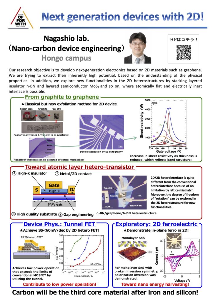
We focus on 2-dimensional (2D) layered electronic devices as one of the most promising future options to enhance the device performance. Although 2D heterointerface is ideally expected to be electrically inert, the superior interface properties are blinded by the imperfection of 2D materials and the interaction with the surroundings. The key to improve the properties is to understand the interface properties between 2D layered materials and the surroundings and to control them from the viewpoint of material science as well as device physics.
Selected Publications
- Y.-R. Chang, R. Nanae, S. Kitamura, T. Nishimura, H. Wang, Y. Xiang, K. Shinokita, K. Matsuda, T. Taniguchi, K. Watanabe, and K. Nagashio, “Shift current photovoltaics based on a noncentrosymmetric phase in in-plane ferroelectric SnS”, Adv. Mater., 2023, 35, 2301172.
- W. Nishiyama, T. Nishimura, K. Ueno, T. Taniguchi, K. Watanabe, and K. Nagashio, “Quantitative Determination of Contradictory Band Gap Values of Bulk PdSe2 from Electrical Transport Properties”, Adv. Funct. Mater., 2022, 32, 2108061.
- T. Sasaki, K. Ueno, T. Taniguchi, K. Watanabe, T. Nishimura, K. Nagashio, “Material and Device Structure Designs for 2D Memory Devices Based on the Floating Gate Voltage Trajectory”, ACS nano, 2021, 15, 6658.
- N. Higashitarumizu, H. Kawamoto, C.-J. Lee, B. -H. Lin, F. -H. Chu, I. Yonemori, T.i Nishimura, K. Wakabayashi, W. -H. Chang & K. Nagashio, “Purely in-plane ferroelectricity in monolayer SnS at room temperature”, Nature commun.,2020, 11, 2428.
- N. Fang, S. Toyoda, T. Taniguchi, K. Watanabe, and K. Nagashio, “Full energy spectra of interface state densities for n– and p-type MoS2 field-effect transistors”, Adv. Func. Mater. 2019, 29, 1904465.

